Manufacturing Process
MOCVD Epitaxy
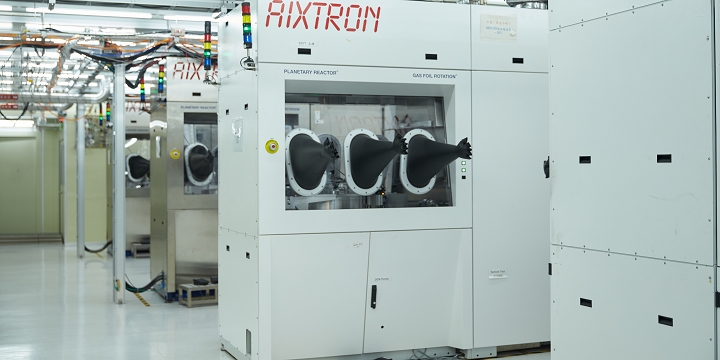
MOCVD
Metal-Organic Chemical Vapor Deposition (MOCVD) is a critical semiconductor thin-film deposition technology. The core principle involves the use of metal-organic compounds and other reactive gases in the vapor phase, which undergo chemical reactions on the substrate surface at high temperatures, leading to the deposition of high-quality crystalline films. MOCVD is widely used in the manufacturing of optoelectronic devices such as Light Emitting Diodes (LEDs), Laser Diodes, High-Speed Transistors, and Solar Cells.
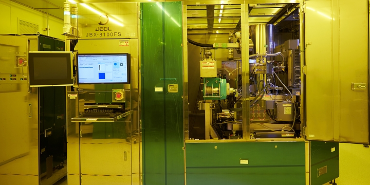
E-Beam Writer
An E-Beam Writer uses a precisely controlled focused electron beam to directly write pre-designed patterns onto the surface of a wafer coated with an electron resist. The pattern is then transferred to the wafer via etching or deposition processes. This technology is widely used in semiconductor lasers and micro-nano fabrication fields.
Wafer Manufacturing
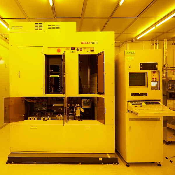
Lithography - Mask Aligner Stepper (4")
Achieving more exposure accuracy by using high accuracy optical and step system to move on wafer to process exposure.
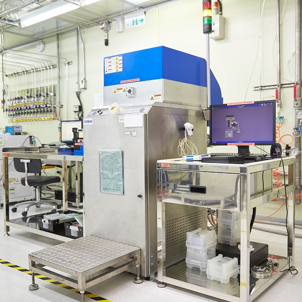
Thin film - PECVD
Using plasma to dissociate the reaction gas and cause it to undergo a chemical reaction then deposition on wafer surface to form a thin film.
PECVD: Plasma Enhanced Chemical Vapor Deposition
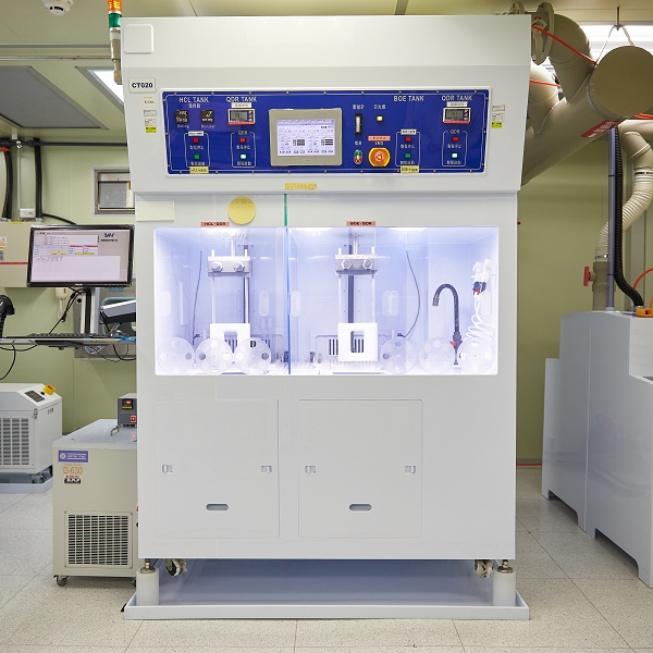
Etch - Auto Wet Bench
Put the wafer in tank of acid, alkaline or organic solutions, using chemical corrosion to process etching.
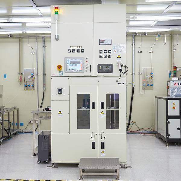
Furnace - Vertical Furnace
Put the wafer in the vertical quartz tube to process oxidation by control temperature and moisture to fine tune.
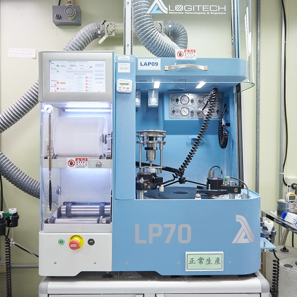
Lapping - Wafer Thinning
The process reduces the thickness of the wafer by grinding.
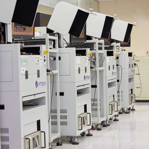
Die Testing
Each die (chip) on the wafer is tested and classified based on its optoelectronic properties.
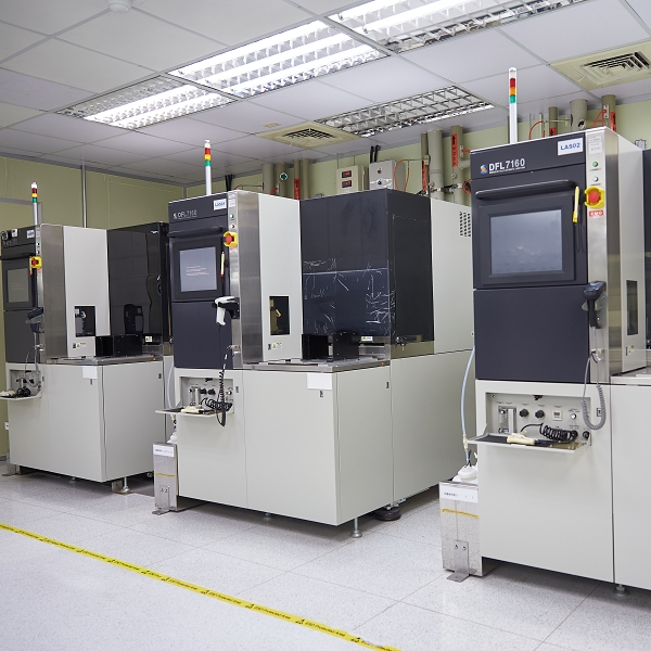
Wafer Dicing
Use a die saw or laser beam to separate the wafer into individual dies.
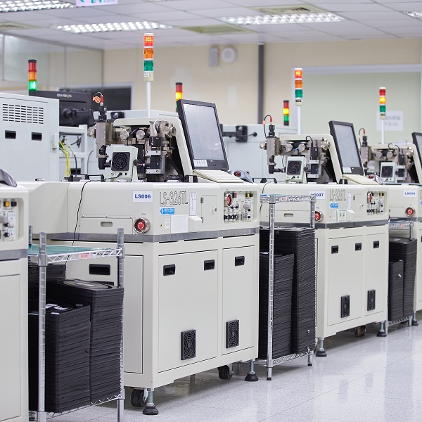
Sorting
Based on the die testing data, the chips are categorized and selected accordingly.
TO-Can Package Assembly
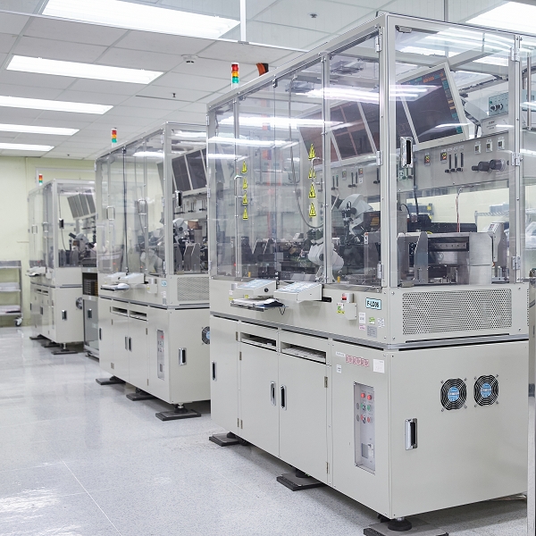
Die Bonding
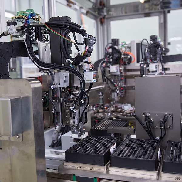
Through the pattern recognition system, the robotic arm accurately places the die (chip) to the designated position.
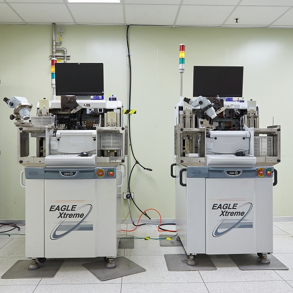
Wire Bonding
The gold wire through heat, pressure and ultrasonic bonds on the die (chip) to the external conductive pins, transmitting the internal signals to the external circuit.
Capping
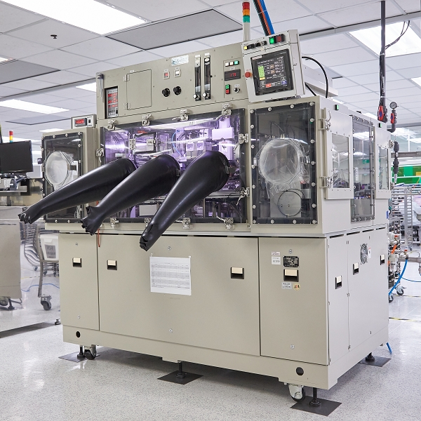
To seal the cap and header using the resistance welder. To prevent gas or liquid entering the component.
Component Testing
The component undergoes optical, electrical, or environmental testing to ensure it meets specifications.
COB (Chip-On-Board) Packaging
Die Bonding
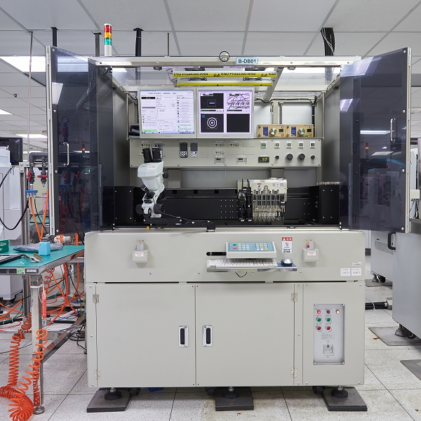
Through the image recognition system, the robotic arm accurately attaches the die (chip) and IC to the designated position of the circuit board (PCBA).
Wire bonding
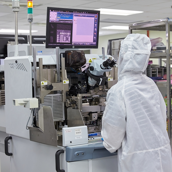
Gold wires are used to connect the contacts on the die (chip) and IC to the circuit board through heat, pressure and ultrasound.
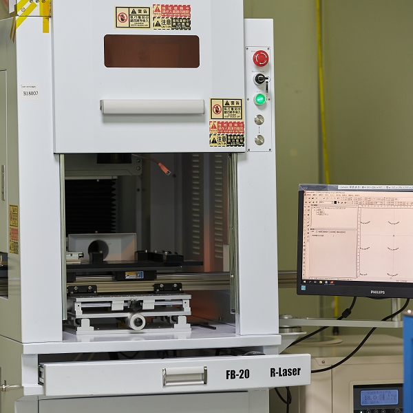
Laser Cutting
Using laser beams, the COB (Chip-On-Board) packaged circuit board (PCBA) is divided into individual optoelectronic modules (OE Modules).
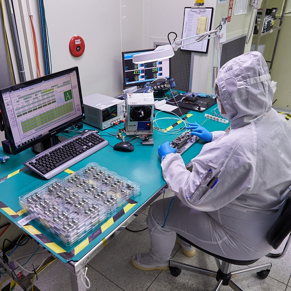
Testing
The optoelectronic modules are connected to a standard light source and powered on to test if their characteristics meet the required specifications.
Sub-Module Assembly (OSA)
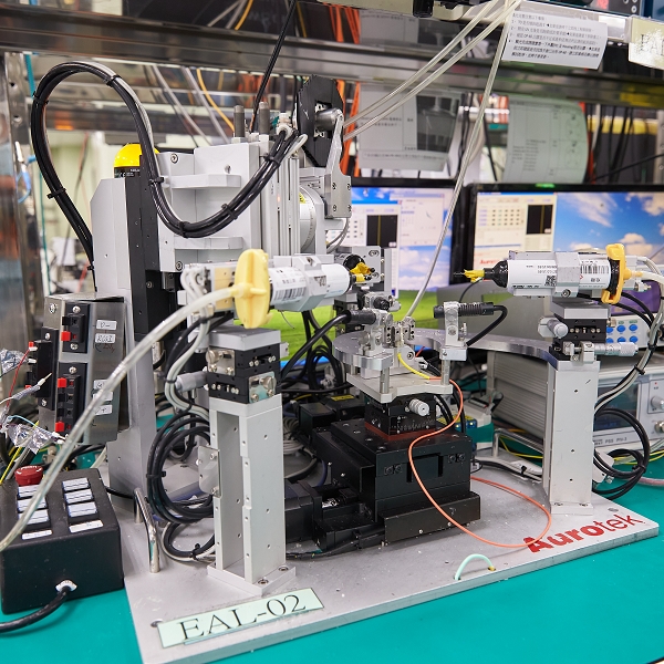
Alignment
After automatically searching for the TO's optimal optical response position, UV curing adhesive is used to temporarily fix the component and fiber optic connector.
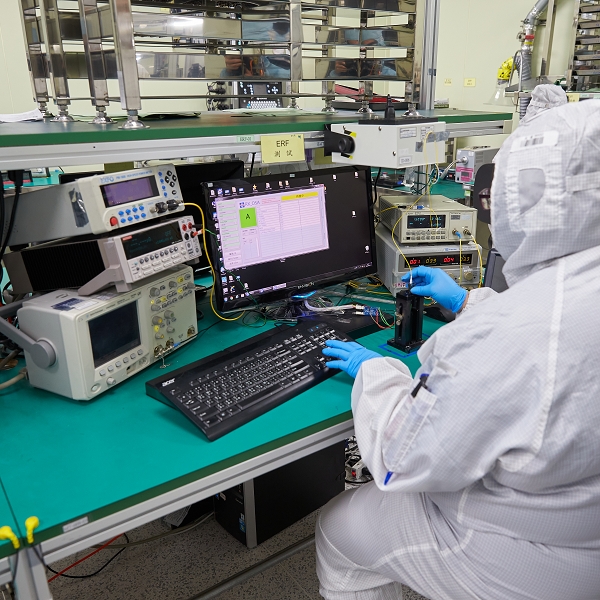
Component Testing
Provide components with optical light or electricity to detect whether the product meets the specifications.To screen out good products and eliminate defective products.
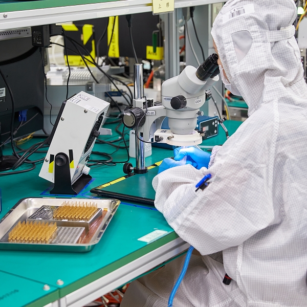
Gluing
An adhesive is used to permanently fix the component (TO) and fiber optic connector.
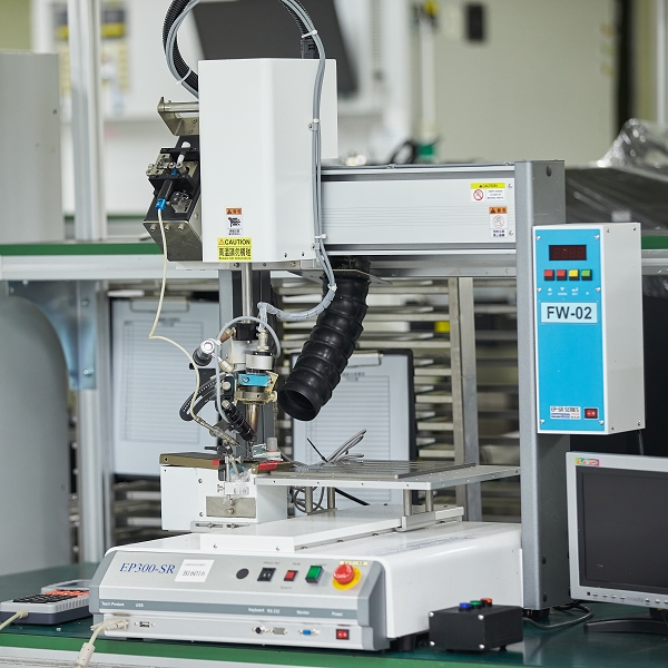
Soldering
A soldering iron is used to heat and apply solder to attach the component to the designated circuit board or connecting cable.


