Wafer Process
Product Number:OEM-CHIP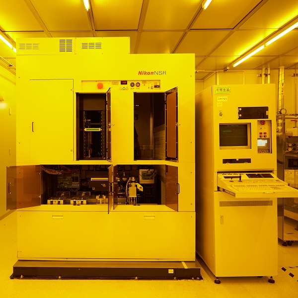
Lithography - Mask Aligner Stepper (4")
Achieving more exposure accuracy by using high accuracy optical and step system to move on wafer to process exposure.
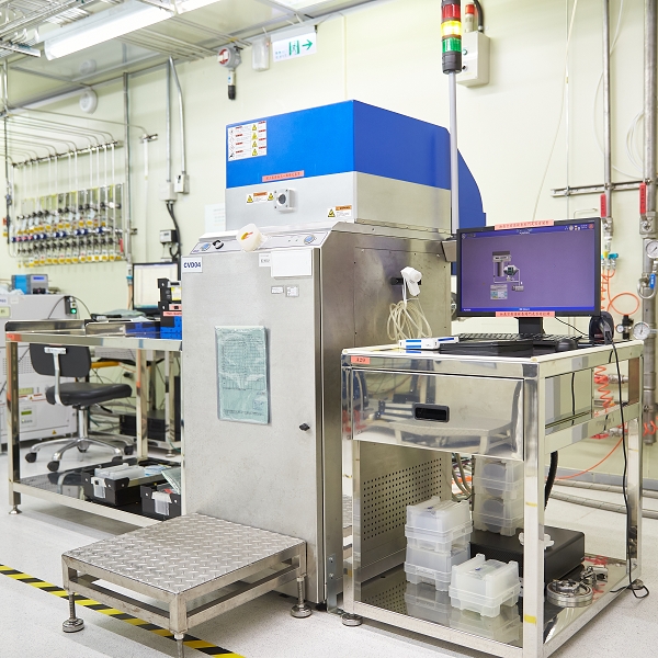
Thin film - PECVD
Using plasma to dissociate the reaction gas and cause it to undergo a chemical reaction then deposition on wafer surface to form a thin film.
PECVD: Plasma Enhanced Chemical Vapor Deposition
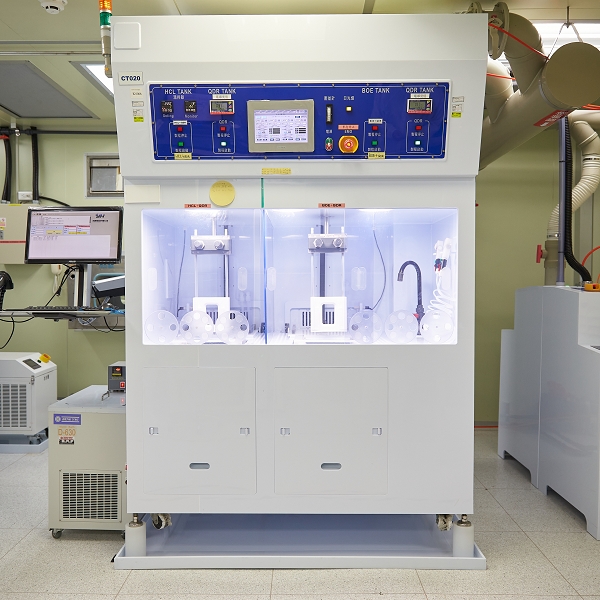
Etch - Auto Wet Bench
Put the wafer in tank of acid, alkaline or organic solutions, using chemical corrosion to process etching.
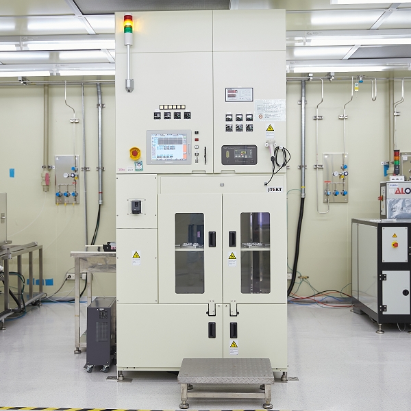
Furnace - Vertical Furnace
Put the wafer in the vertical quartz tube to process oxidation by control temperature and moisture to fine tune.
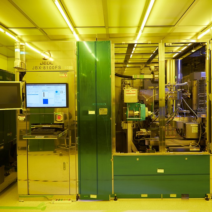
E-Beam Writer
An E-Beam Writer uses a precisely controlled focused electron beam to directly write pre-designed patterns onto the surface of a wafer coated with an electron resist. The pattern is then transferred to the wafer via etching or deposition processes. This technology is widely used in semiconductor lasers and micro-nano fabrication fields.
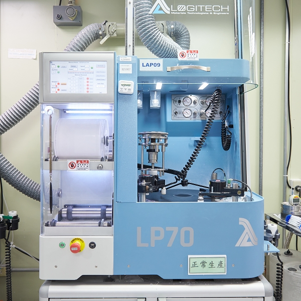
Lapping - Wafer Thinning
The process reduces the thickness of the wafer by grinding.


